Tungsten Filament Scanning Electron Microscope | SEM2000
Home > Products > Tungsten Filament Scanning Electron Microscope | SEM2000
The CIQTEK SEM2000 is a basic and versatile analytical tungsten filament scanning electron microscope with 20 kV resolution up to 3.9 nm and support for upgrading to 30 kV, allowing observation of microstructural information of sub-microscale samples.
It has a larger range of motion than a desktop / benchtop SEM and is suitable for rapid screening of samples, and has more expansion interfaces for BSED, EDS/EDX, and other accessories to enable a wider range of applications.
Accesories
- Autosampler AS-500 with optional rinse station Argon humidifier.
- Introduction system kits for improved performance (small volume, organics, Hydrofluoric acid, high total dissolved solids).
- Concomitant Metals Analyzer for simultaneous measurement of hydride forming elements and other elements.
- Oxygen kit for alkali elements in organics.
Features
Optical Navigation
- Easy to navigate by clicking where you want to see. Standard optical navigation camera for high-definition sample stage photos and quick sample positioning.
Anti-collision
- More novice-friendly anti-collision design for maximum protection of sensitive units.
One-Click Imaging
- *The software is easy to operate with one-click imaging.
Working Distance
- The optimal analysis distance and image distance are two in one to easily experience quality performance.
Specifications
- Resolution : 3.9 nm @ 20 kV
- Acceleration Voltage : 0.5 ~ 20 kV (30 kV optional)
- Magnification : 1 ~ 300,000x
Applications
Microstructure of endosperm starch granules of new rice
Acceleration voltage: 10 kV / Magnification: ×5000
Salt
Acceleration voltage: 1 kV / Magnification: ×2000
Fiber cross-section
Acceleration voltage: 7 kV / Magnification: ×1000
Polymer lens arrays Acceleration voltage: 15 kV / Magnification: ×200
Parameters
| Electro-Optical Systems | Electron Gun | Pre-aligned medium-sized fork-type tungsten filament |
| Resolution | 3.9 nm @ 20 kV (SE) | |
| 4.5 nm @ 20 kV (BSE) | ||
| Magnification | 1 x~300,000 x | |
| Acceleration Voltage | 0.5 kV ~ 20 kV | |
| Imaging Systems | Detector | 
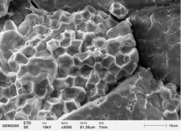
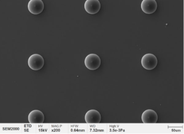
Secondary Electron Detector (ETD) |
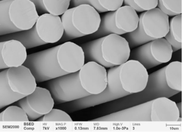
| *Backscattered electron detector (BSED), *energy spectrometer EDS, etc. | ||
| Image Format | TIFF, JPG, BMP, PNG | |
| Vacuum System | High Vacuum | Better than 5×10⁻⁴ Pa |
| Control Mode | Fully automated control system | |
| Pumps | Mechanical Pump ×1, Molecular Pump ×1 | |
| Sample Chamber | Camera | Optical Navigation |
| Sample Table | Two-axis automatic | |
| Distance | X: 100 mm | |
| Y: 100 mm | ||
| Software | Operating System | Windows |
| Navigations | Optical Navigation, Gesture Quick Navigation | |
| Automatic Functions | Auto Brightness Contrast, Auto Focus, Automatic Dissipation | |
| Special Functions | Intelligent Assisted Dispersion, *Large-Scale Image Stitching (Optional accessories) | |
| Installation Requirements | Space | L ≥ 3000 mm, W ≥ 4000 mm, H ≥ 2300 mm |
| Temperature | 20°C (68°F) ~ 25°C (77°F) | |
| Humidity | ≤ 50 % | |
| Power Supply | AC 220 V(±10 %), 50 Hz, 2 kVA |